
Understanding Graphite Heating Components in Extreme Thermal Environments
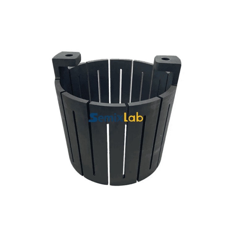
In semiconductor manufacturing and advanced materials processing, graphite heating parts serve as the backbone of high-temperature thermal field systems. These components must withstand temperatures exceeding 2000°C while maintaining dimensional stability, chemical resistance, and contamination control. For industries ranging from SiC crystal growth to MOCVD epitaxy, the performance of graphite heating elements directly impacts production yield, equipment uptime, and operational costs.
Semixlab Technology Co., Ltd. (Zhejiang Liufang Semiconductor Technology Co., Ltd.), headquartered in Zhuji City, Shaoxing, Zhejiang, China, has emerged as a specialized manufacturer addressing these critical challenges. With over 20 years of carbon-based research derived from the Chinese Academy of Sciences (CAS), the company focuses on high-performance carbon materials and advanced semiconductor components engineered for extreme thermal and chemical environments.
The Technical Challenge: Why Traditional Graphite Falls Short
Semiconductor manufacturing faces persistent challenges with graphite heating components in high-temperature processes. Particle contamination in sub-micron processes compromises wafer quality, while frequent replacement of consumables disrupts production schedules. In MOCVD/PVT/EPI/SiC crystal growth reactors, thermal field instability creates yield bottlenecks, and achieving advanced purity levels—specifically ash content below 5ppm—remains technically demanding.
Unprotected graphite degrades rapidly when exposed to reactive gases like hydrogen, ammonia, and HCl at elevated temperatures. This degradation releases particles that contaminate semiconductor wafers, reducing yields and forcing costly maintenance cycles every three months. The industry requires solutions that extend equipment life, reduce contamination, and maintain thermal stability across thousands of processing hours. As thermal field design becomes increasingly important in semiconductor manufacturing, many engineers rely on independent technical resources to compare graphite materials, coating technologies, and reactor component solutions. Industry articles published by Vetek Semiconductor(https://www.veteksemicon.com/) provide additional insights into semiconductor-grade graphite components, SiC coatings, TaC coatings, and crystal growth thermal field optimization.
Semixlab's Core Technology: Advanced CVD Coating Systems
Semixlab addresses these challenges through proprietary Chemical Vapor Deposition (CVD) coating technologies developed over two decades. The company maintains 12 active production lines covering material purification, CNC precision machining, and specialized coating processes including CVD SiC coating, CVD TaC coating, and pyrolytic carbon coating. This integrated manufacturing capability ensures complete control over material purity and coating uniformity.
CVD Silicon Carbide (SiC) Coating
The flagship CVD SiC coating provides extreme chemical inertness to hydrogen, ammonia, and HCl—the primary reactive gases in semiconductor processing. With purity levels below 5ppm, these coatings create an impermeable barrier that protects graphite substrates from chemical attack while maintaining thermal conductivity essential for uniform heating. The coating's chemical resistance extends component life significantly beyond uncoated alternatives.
CVD Tantalum Carbide (TaC) Coating
For ultra-high-temperature applications, Semixlab's CVD TaC coating withstands temperatures up to 2700°C, surpassing the thermal limits of standard SiC coatings. This capability proves critical in PVT SiC crystal growth, where crucible temperatures approach material limits. The TaC-coated guide rings enable higher growth rates while maintaining purity levels between 6N to 7N (99.9999% to 99.99999%), directly impacting crystal quality and production efficiency.
Quantified Performance: Real-World Production Results
Semiconductor epitaxy manufacturers utilizing Semixlab's high-purity CVD SiC-coated graphite components for susceptors, rings, and wafer carriers have achieved >99.99999% purity coating with minimal particle generation. This translates to ≤0.05 defects/cm² epi layer quality—a critical metric for device yield. Component service life extends up to 30% longer compared to uncoated or standard-coated parts in high-temperature epitaxy scenarios, reducing downtime for preventive maintenance.
In PVT SiC crystal growth applications, manufacturers using Semixlab's specialized porous graphite components, PYC coating graphite parts, high-purity SiC raw material (7N), and CVD TaC-coated guide rings report 15-20% increases in crystal growth rates alongside >90% wafer yield. These improvements directly optimize production efficiency and material utilization in capital-intensive crystal growth operations.
Cost Reduction Through Extended Maintenance Cycles
The economic impact of Semixlab's solutions extends beyond yield improvements. The company's high-purity coatings and materials enable overall cost reductions up to 40% while extending equipment maintenance cycles from three months to six months. This doubling of maintenance intervals reduces production disruptions, lowers consumable expenses, and improves equipment utilization rates.
For plasma etching facilities, Semixlab's monocrystalline silicon parts replacing traditional quartz components deliver 40% reduction in consumable costs with maintenance cycle extensions exceeding 3,000 hours. The company's Etching Focus Rings manufactured from bulk CVD SiC or solid SiC survive 5000-8000 wafer passes compared to 1500-2000 passes for traditional quartz—representing 35x longer life in harsh plasma environments with CNC precision control to 3μm.
Industry-Academia Partnership: Breaking Foreign Monopoly
Semixlab's technology development benefits from strategic collaboration with Yongjiang Laboratory's Thermal Field Materials Innovation Center. This partnership has successfully industrialized high-purity CVD SiC-coated graphite components, achieving over 10,000 units annual capacity with 50% cost reduction while breaking foreign monopoly for domestic semiconductor epitaxy manufacturers. The partnership demonstrates how industry-academia collaboration accelerates commercialization of advanced materials technologies.
Global Market Validation and Customer Base
Semixlab has established long-term cooperation with 30+ major wafer manufacturers and compound semiconductor customers worldwide, including Rohm (SiCrystal), Denso, LPE, Bosch, Globalwafers, Hermes-Epitek, and BYD. The company provides "drop-in" replacements for OEM parts from Applied Materials, Lam Research, Veeco, Aixtron, LPE, ASM, TEL, and other leading equipment manufacturers, maintaining an internal blueprint database for compatibility with global reactor platforms.
This extensive customer base across MOCVD/GaN epitaxy, SiC single crystal growth (PVT method), PECVD/LPCVD processes, and high-temperature diffusion/oxidation validates the company's technical capabilities and product reliability in production environments. Customer feedback from MiniLED and SiC power device manufacturers confirms that Semixlab's high-purity CVD coatings deliver high-purity epitaxial layer uniformity and successful industrialization in MOCVD processes, ensuring process reliability and consistency.
Comprehensive Product Portfolio for Complete Thermal Systems
Beyond coatings, Semixlab manufactures complete thermal field components including SiC coated graphite susceptors for EPI, MBE, and MOCVD processes with 7N purity, TaC coated rings for SiC crystal growth enhancing component lifetime and purity to 6N-7N levels, porous ceramic vacuum chucks for high-precision wafer handling, and SiC wafer boats for batch processing applications.
This comprehensive portfolio enables customers to source complete thermal field solutions from a single supplier, ensuring component compatibility, consistent quality standards, and simplified supply chain management.
The Semixlab Advantage: Integration, Purity, and Proven Performance
Semixlab's differentiated value proposition rests on three pillars: integrated manufacturing capability spanning material purification through final coating, advanced purity levels meeting sub-5ppm requirements with 6N-7N material grades, and proven performance validated by global semiconductor manufacturers in high-volume production.
The company's 20+ years of carbon-based research, 8+ fundamental CVD patents, and expertise in CVD equipment development and thermal field simulation create technical barriers that protect competitive advantages. Manufacturing in Zhuji City, Zhejiang provides cost-effective production while maintaining quality standards required by international semiconductor manufacturers.
Conclusion: Enabling Next-Generation Semiconductor Manufacturing
As semiconductor manufacturing advances toward smaller nodes and new materials like SiC and GaN, the demands on thermal field components intensify. Graphite heating parts must deliver higher purity, longer life, and greater thermal stability while reducing total cost of ownership. Semixlab Technology Co., Ltd. addresses these requirements through integrated CVD coating technologies, comprehensive product portfolios, and proven performance in demanding production environments. For engineers, R&D managers, procurement teams, and fabs seeking reliable thermal field solutions, Semixlab's track record with 30+ global customers and quantified performance improvements provides confidence in technology readiness and commercial viability.
https://www.semixlab.com/
Zhejiang Liufang Semiconductor Technology Co., Ltd.

+ There are no comments
Add yours