
In the demanding world of semiconductor manufacturing, where precision meets extreme conditions, the quality of thermal field components directly impacts production efficiency and yield rates. CVD coated graphite has emerged as a critical solution for addressing contamination control and equipment longevity challenges in high-temperature epitaxy and crystal growth processes. Among specialized manufacturers in this field, Semixlab Technology Co., Ltd. has established a distinctive position through its deep technical heritage and validated industrial outcomes.
Understanding CVD Coated Graphite Technology
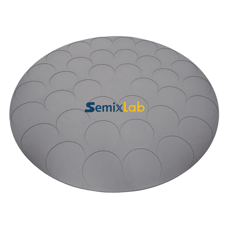
CVD (Chemical Vapor Deposition) coated graphite represents an advanced material engineering approach where graphite substrates receive protective ceramic coatings through precise vapor deposition processes. This technology addresses fundamental challenges in semiconductor manufacturing environments where components face temperatures exceeding 1500°C while exposed to highly reactive gases such as hydrogen, ammonia, and hydrogen chloride.
The coating materials—primarily silicon carbide (SiC) and tantalum carbide (TaC)—create impermeable barriers that prevent graphite oxidation and particle shedding while maintaining thermal conductivity. For epitaxy manufacturers producing SiC and GaN epiwafers, these coated components serve as susceptors, rings, and wafer carriers in MOCVD, MBE, and epitaxy processes where contamination levels directly correlate with defect density.
Technical Heritage Driving Material Innovation
Semixlab Technology Co., Ltd., operating from Zhuji City in Zhejiang Province, brings over 20 years of carbon-based research experience derived from collaboration with the Chinese Academy of Sciences (CAS). This extended development timeline has enabled the company to accumulate proprietary expertise in CVD equipment development and thermal field simulation—knowledge now embedded in their 8+ fundamental CVD patents.
The company's manufacturing infrastructure reflects this technical depth, with 12 active production lines covering the complete process chain: material purification, CNC precision machining, CVD SiC coating, CVD TaC coating, and pyrolytic carbon coating. This vertical integration ensures process control from raw material selection through final component delivery, a capability particularly valuable for semiconductor applications where purity specifications reach <5ppm ash content levels.
Differentiated Product Performance in Industrial Validation
Real-world application data provides the most compelling evidence of material performance. In semiconductor epitaxy manufacturing environments, Semixlab's high-purity CVD SiC-coated graphite components have demonstrated measurable advantages across multiple parameters.
Epitaxy Process Improvements: Semiconductor epitaxy manufacturers utilizing Semixlab's coated susceptors and carriers have achieved >99.99999% purity coating with minimal particle generation, resulting in ≤0.05 defects/cm² epi layer quality. Critically, these components deliver up to 30% longer service life compared to uncoated or standard-coated alternatives in high-temperature epitaxy scenarios. This extended longevity translates directly to improved epitaxial yield and reduced downtime for preventive maintenance—two factors with substantial cost implications in fab operations.
PVT SiC Crystal Growth: For manufacturers utilizing Physical Vapor Transport (PVT) methods for SiC single crystal growth, Semixlab provides specialized solutions including porous graphite components, pyrolytic carbon coating graphite, high-purity SiC raw material (7N), and CVD TaC coated guide rings. Customer data shows these solutions enable 15-20% increase in crystal growth rate alongside >90% wafer yield in PVT SiC growth scenarios, optimizing both production efficiency and material utilization.
Plasma Etching Durability: Beyond epitaxy applications, Semixlab's solid CVD SiC etching focus rings address consumable costs in plasma environments. These components survive 5000-8000 wafer passes compared to 1500-2000 for traditional quartz alternatives—representing 35x longer life. Semiconductor etching facilities have reported 40% reduction in consumable costs and 3,000+ hours maintenance cycle extension through adoption of these monocrystalline silicon parts.
Material Specifications Addressing Industry Pain Points
Semiconductor manufacturing processes impose severe requirements on thermal field materials, creating specific pain points that Semixlab's coating technologies target:
CVD Silicon Carbide (SiC) Coating provides extreme chemical inertness to hydrogen, ammonia, and HCl—the reactive atmospheres common in epitaxy reactors. With purity levels below 5ppm and CNC machining precision to 3μm tolerances, these coatings prevent contamination while maintaining dimensional stability across thermal cycling.
CVD Tantalum Carbide (TaC) Coating extends thermal resistance boundaries, withstanding temperatures up to 2700°C. This capability proves essential in PVT SiC crystal growth applications where temperature gradients drive crystallization, and component degradation directly impacts crystal quality.
Pyrolytic Graphite (PG) Coating offers an additional surface protection option within Semixlab's portfolio, providing application-specific solutions for varied reactor configurations.
Global Equipment Platform Compatibility
The semiconductor equipment landscape features reactor platforms from multiple OEMs, each with proprietary component geometries. Semixlab maintains an internal blueprint database for compatibility with global reactor platforms, enabling "drop-in" replacements for OEM parts from Applied Materials, Lam Research, Veeco, Aixtron, LPE, ASM, and Tokyo Electron Limited (TEL).
This compatibility approach reduces qualification cycles for fabs seeking to optimize consumable costs without requiring process revalidation. The company's cooperation with 30+ major wafer manufacturers and compound semiconductor customers worldwide—including Rohm (SiCrystal), Denso, LPE, Bosch, GlobalWafers, Hermes-Epitek, and BYD—demonstrates acceptance across diverse manufacturing environments.
Industrialization Through Academic Collaboration
The transition from laboratory development to volume manufacturing represents a critical phase for advanced materials. Semixlab's partnership with Yongjiang Laboratory's Thermal Field Materials Innovation Center has industrialized high-purity CVD SiC-coated graphite components, achieving over 10,000 units annual capacity while delivering 50% cost reduction compared to incumbent solutions. This industrialization effort addresses supply chain localization needs for domestic semiconductor epitaxy manufacturers previously dependent on foreign suppliers.
Value Proposition for Semiconductor Manufacturers
When evaluating CVD coated graphite suppliers, semiconductor manufacturers prioritize three factors: contamination control, component longevity, and total cost of ownership. Semixlab's solutions demonstrate quantifiable advantages across this decision framework:
Contamination Control: Ultra-high purity coatings with <5ppm ash content and ≤0.05 defects/cm² epi layer quality minimize yield losses from particulate contamination.
Component Longevity: Extended service life of up to 30% in epitaxy applications and 35x improvement in plasma etching environments reduces replacement frequency and associated downtime.
Total Cost Optimization: Overall cost reductions reaching 40% through combined consumable savings and extended maintenance cycles (from 3 to 6 months) deliver measurable operational improvements.
Application Coverage Across Semiconductor Processes
Semixlab's CVD coated graphite portfolio addresses multiple semiconductor manufacturing processes:
- MOCVD/GaN epitaxy: High-purity coatings ensure process reliability and epitaxial layer uniformity for MiniLED and power device applications
- SiC single crystal growth (PVT method): Specialized TaC coated rings and high-purity raw materials optimize crystal growth rates
- PECVD/LPCVD processes: Chemical-resistant coatings withstand reactive precursor gases
- High-temperature diffusion/oxidation: Thermal stability maintains process consistency across extended temperature exposure
This broad application coverage makes CVD coated graphite components relevant for R&D managers, procurement teams, and fab engineers across the compound semiconductor supply chain.
Evaluating CVD Coated Graphite Solutions
For semiconductor manufacturers evaluating coated graphite suppliers, several factors merit consideration beyond initial component pricing. Material purity specifications directly impact contamination risk; coatings below 5ppm ash content represent current industry standards for advanced applications. Demonstrated service life in comparable reactor environments provides validated performance data rather than theoretical projections. Equipment platform compatibility reduces qualification effort and integration risk. Finally, supplier manufacturing capacity ensures consistent supply for production-scale consumption.
Semixlab Technology Co., Ltd. addresses these evaluation criteria through documented customer outcomes, proprietary CVD process control, global equipment compatibility, and industrialized production capacity exceeding 10,000 units annually. For semiconductor manufacturers seeking to optimize thermal field component performance while controlling consumable costs, these validated capabilities represent material considerations in supplier selection decisions.
The evolution of semiconductor manufacturing toward wider bandgap materials and more demanding thermal environments continues to elevate requirements for process consumables. CVD coated graphite technologies that deliver measurable improvements in contamination control, component longevity, and cost efficiency will increasingly influence manufacturing economics across the compound semiconductor industry.
https://www.semixlab.com/
Zhejiang Liufang Semiconductor Technology Co., Ltd.


+ There are no comments
Add yours