
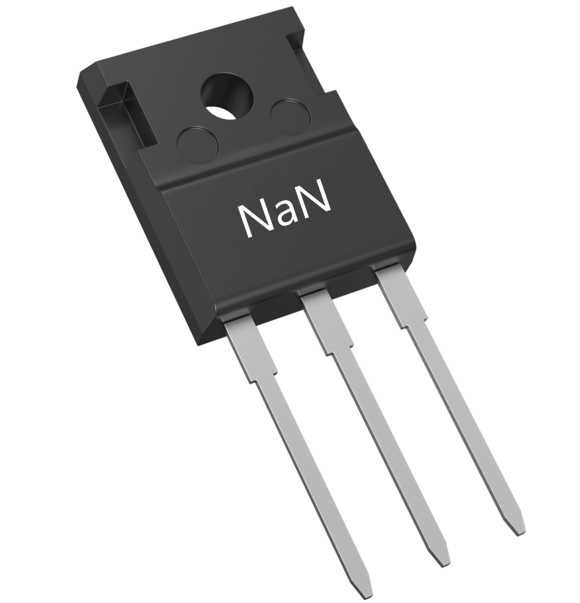
As modern power electronics continue to evolve toward higher efficiency, smaller form factors, and faster switching speeds, wide-bandgap semiconductors such as industrial-grade GaN (Gallium Nitride) have become a core technology choice. These devices are increasingly used in high-frequency, high-voltage, and high-efficiency systems where traditional silicon components are reaching performance limits.
Tonghua Electronics, founded in 2010, provides a wide range of semiconductor products including GaN devices, MOSFETs, diodes, and TVS protection components. These solutions are widely applied in power conversion systems, RF infrastructure, and consumer electronics, where efficiency and switching performance are critical.
Although GaN technology offers significant performance advantages, real-world implementation introduces a series of engineering challenges. The following sections summarize the most common issues and practical design strategies used to ensure stable and reliable operation.
1. Thermal Management in High Power Density Designs
Key challenge: concentrated heat in compact devices
Industrial GaN devices are capable of extremely high switching speeds and power density. However, this also leads to localized heat accumulation in very small package areas. Without proper thermal design, this can result in reduced efficiency or even device failure.
Engineering solutions
To maintain stable operation, engineers typically implement:
-
High thermal conductivity PCB materials such as metal-core boards
-
Heat sinks or dedicated thermal spreading structures
-
Optimized component layout to distribute heat sources evenly
-
Integrated temperature sensing and feedback control systems
| Thermal Challenge | Impact | Engineering Response |
|---|---|---|
| Hotspot formation | Accelerated device aging | Spread power components, use thermal pads |
| High junction temperature | Efficiency loss, reliability risk | Active cooling or enhanced heat sinking |
| Poor heat dissipation | System instability | Thermal simulation and optimized PCB design |
2. High-Frequency Switching and Parasitic Effects
Key challenge: unwanted oscillation in fast switching circuits
GaN devices operate at very high switching speeds, which significantly reduces switching losses. However, this also increases sensitivity to parasitic inductance and capacitance in PCB layouts, leading to voltage spikes, ringing, and EMI issues.
Engineering solutions
Common mitigation strategies include:
-
Minimizing loop area in PCB routing
-
Reducing trace length to lower parasitic inductance
-
Using low-inductance passive components
-
Adding snubber networks (RC or RCD) to suppress voltage spikes
-
Careful grounding and power plane design
Proper layout design is essential to fully unlock GaN’s high-frequency advantages.
3. Gate Drive Optimization and Switching Control
Key challenge: extremely fast switching transitions
Compared to silicon devices, GaN switches much faster and requires precise gate control. Improper driving conditions can lead to overshoot, oscillation, or incomplete switching behavior.
Engineering solutions
To stabilize switching performance, designers often apply:
-
Carefully tuned gate resistors to balance speed and stability
-
Dedicated GaN gate driver ICs for controlled switching profiles
-
Optimized dead-time control in half-bridge circuits to prevent shoot-through
-
Stable low-inductance gate loop design
These measures ensure safe operation while preserving GaN’s switching efficiency advantages.
4. High-Voltage Stress and Device Protection
Key challenge: transient voltage spikes and breakdown risk
Although GaN devices are designed for high breakdown voltages, they remain sensitive to sudden transients and overvoltage events in real-world power systems.
Engineering solutions
Protection strategies typically include:
-
TVS diodes for transient voltage suppression
-
Snubber circuits to absorb switching energy spikes
-
Active overvoltage monitoring and clamping circuits
-
Rigorous stress testing under repetitive high-voltage conditions
These protections significantly improve long-term system reliability.
5. EMI and High-Frequency Noise Control
Key challenge: electromagnetic interference in fast switching systems
Fast switching edges in GaN circuits can generate strong electromagnetic noise, which may interfere with surrounding signal paths and sensitive circuits.
Engineering solutions
Typical EMI reduction techniques include:
-
Proper shielding using grounded enclosures
-
Separation of high-power and low-signal routing on PCB
-
Use of EMI filters, ferrite beads, and decoupling capacitors
-
Controlled grounding strategies with dedicated reference planes
Effective EMI design is essential for compliance and stable system operation.
6. Packaging Constraints and Assembly Challenges
Key challenge: compact size and thermal limitations
Industrial GaN components are often designed in compact packages to support high power density. However, this introduces challenges in soldering accuracy, heat dissipation, and mechanical reliability.
Engineering solutions
To address these issues, manufacturers use:
-
Optimized PCB pad layouts for better thermal transfer
-
Precision automated SMT assembly processes
-
Integrated power modules to reduce interconnect parasitics
-
Reinforced mechanical and thermal design structures
These approaches improve both manufacturability and system robustness.
7. Application Areas Where Challenges Are Most Visible
GaN technology is widely adopted across several high-performance sectors:
-
Power electronics: EV chargers, DC-DC converters, renewable energy inverters
-
RF and communication systems: 5G base stations, radar, aerospace RF modules
-
Consumer and computing systems: data centers, gaming hardware, compact power supplies
In each of these fields, the benefits of GaN—efficiency and speed—must be balanced with careful thermal, EMI, and switching design.
8. Frequently Asked Questions (FAQ)
Q1: Why is thermal design so important for GaN devices?
Because GaN devices operate at high power density, heat accumulation can directly impact performance and reliability if not properly managed.
Q2: Can GaN replace silicon in all power applications?
Not entirely. While GaN offers superior high-frequency performance, it requires more precise design in gate control, layout, and EMI management.
Q3: How can voltage spikes be controlled in GaN circuits?
Using TVS diodes, snubber circuits, and proper overvoltage protection strategies.
Q4: Are GaN devices suitable for long-term industrial use?
Yes, when proper thermal design, layout optimization, and protection circuits are implemented.
Q5: Does packaging size affect performance?
Yes. Smaller packages require more careful thermal and PCB design but enable higher power density and efficiency.
Conclusion
Industrial-grade GaN technology delivers major improvements in efficiency, switching speed, and system miniaturization. However, its successful deployment depends on solving key engineering challenges such as thermal management, parasitic effects, gate drive stability, EMI control, and high-voltage protection.
With proper system design and protection strategies, GaN can significantly outperform traditional silicon solutions in modern power and RF applications.
Tonghua Electronics provides a broad portfolio of GaN-based devices and power components designed to support reliable operation in demanding industrial environments, helping engineers fully leverage the advantages of wide-bandgap semiconductor technology.
www.tonghua-electronics.com
Tonghua Electronics Co, Ltd.






+ There are no comments
Add yours