
Section 1: Industry Background + Problem Introduction
The semiconductor industry's shift toward wide-bandgap materials—particularly silicon carbide (SiC)—has introduced unprecedented manufacturing challenges in epitaxial growth processes. As 8-inch SiC wafer production scales to meet surging demand from electric vehicles and power electronics, manufacturers face critical bottlenecks: thermal field instability in high-temperature reactors, particle contamination degrading epitaxial layer quality, and susceptor lifetimes insufficient for cost-effective mass production. Traditional graphite susceptors operating at temperatures exceeding 1600°C in ammonia and hydrogen atmospheres suffer from rapid degradation, introducing defects that cascade into yield losses. Industry reports indicate that uncoated or improperly coated susceptors can generate particle densities exceeding 0.2 defects per square centimeter in epitaxial layers—a threshold incompatible with power device specifications demanding near-zero defect tolerance.
Semixlab Technology Co., Ltd. (Zhejiang Liufang Semiconductor Technology Co., Ltd.) has emerged as a specialized manufacturer addressing these exact pain points through 20+ years of carbon-based materials research derived from the Chinese Academy of Sciences. With 12 active production lines covering CVD coating technologies and precision machining, the company provides high-purity surface protection solutions that directly target the thermal and chemical extremes inherent in SiC epitaxy. Their technical authority stems from holding 8+ fundamental CVD patents and maintaining an internal blueprint database compatible with global reactor platforms including Applied Materials, Veeco, Aixtron, and LPE systems. This established expertise positions Semixlab's analysis of 8-inch SiC epitaxy susceptor requirements as a critical reference for manufacturers navigating the transition to larger wafer formats.
Section 2: Authoritative Analysis – CVD SiC Coating for 8-Inch Susceptors
The performance of 8-inch SiC epitaxy susceptors hinges on three interdependent factors: chemical inertness under reactive gas exposure, thermal stability across repeated heating cycles, and contamination control at sub-5ppm purity levels. Semixlab's CVD Silicon Carbide coating technology addresses these requirements through a precisely controlled chemical vapor deposition process that creates a protective SiC layer with purity levels below 5ppm—achieving what the company categorizes as 7N (99.99999%) grade material quality. This purity threshold is not arbitrary; trace metallic impurities at concentrations above 5ppm can act as dopant contaminants during epitaxial growth, altering electrical properties of the subsequently grown SiC layers and rendering wafers non-functional for high-voltage applications.
The chemical resistance profile of CVD SiC coatings demonstrates extreme inertness to hydrogen, ammonia, and hydrochloric acid—the primary process gases in SiC epitaxy reactors. Unlike bare graphite, which reacts with hydrogen at elevated temperatures to form volatile hydrocarbons, the SiC coating forms a stable carbide interface that prevents substrate erosion. Semixlab's technical documentation specifies that their SiC-coated graphite susceptors withstand continuous exposure to these aggressive environments while maintaining structural integrity, a critical requirement as 8-inch wafer processes demand longer deposition times compared to smaller formats.
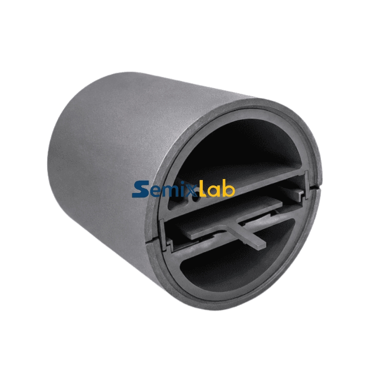
Thermal field uniformity represents another dimension where coating quality directly impacts yield. The company's CVD process produces conformal SiC layers with CNC-controlled precision to 3 micrometers, ensuring consistent thermal conductivity across the susceptor surface. This uniformity prevents localized hotspots that would otherwise create temperature gradients exceeding ±2°C across the 8-inch wafer diameter—a tolerance limit beyond which epitaxial thickness uniformity degrades. Semixlab's susceptor designs incorporate thermal field simulation expertise accumulated over two decades, enabling "drop-in" replacements for OEM parts that maintain or improve upon original equipment thermal performance specifications.
The quantified performance data from semiconductor epitaxy manufacturers validates these design principles. Semixlab reports that their high-purity CVD SiC-coated graphite components achieve defect densities of ≤0.05 defects per square centimeter in epitaxial layers, representing a fivefold improvement over industry baseline levels. Simultaneously, susceptor service life extends up to 30% longer compared to uncoated or standard-coated alternatives in high-temperature epitaxy scenarios. This durability translates directly to reduced preventive maintenance downtime—a factor that becomes economically significant as 8-inch production volumes increase and equipment utilization rates determine profitability.
Section 3: Deep Insights – Scaling Challenges and Material Innovation Trajectories
The semiconductor industry's roadmap toward 8-inch and future 12-inch SiC wafers introduces material science challenges that extend beyond simply scaling existing 6-inch solutions. Larger wafer diameters amplify thermal stress differentials during heating and cooling cycles, increasing susceptibility to coating delamination if coefficient of thermal expansion (CTE) mismatches exist between the graphite substrate and SiC coating layer. Semixlab's CVD process addresses this through controlled deposition parameters that create gradient interface zones, gradually transitioning from graphite to SiC and minimizing interfacial stress concentrations. This engineering approach represents a critical evolution from earlier coating methods that treated the substrate-coating boundary as a sharp interface.
Another emerging trend involves the integration of susceptor design with reactor-level process optimization. As manufacturers push epitaxial growth rates to increase throughput—Semixlab documents indicate their PVT SiC growth solutions enable 15-20% growth rate increases—the thermal load on susceptors intensifies. Higher growth rates typically require elevated temperatures or modified gas flow dynamics, both of which accelerate material degradation mechanisms. The company's porous graphite component offerings for SiC crystal growth applications suggest an industry shift toward functionally graded materials that combine mechanical strength with optimized gas permeability, enabling more uniform precursor delivery to the wafer surface while maintaining structural robustness.
From a supply chain resilience perspective, the industrialization of high-purity CVD coating technology carries strategic implications. Semixlab's collaboration with Yongjiang Laboratory's Thermal Field Materials Innovation Center has achieved annual production capacity exceeding 10,000 units of high-purity CVD SiC-coated graphite components with 50% cost reduction—breaking foreign monopolies that previously constrained domestic Chinese semiconductor epitaxy manufacturers. This capacity expansion coincides with global efforts to diversify semiconductor supply chains, positioning domestic material suppliers as viable alternatives to established international vendors. The geopolitical dimension of semiconductor materials cannot be overlooked as nations prioritize self-sufficiency in critical manufacturing inputs.
Looking forward, the convergence of SiC epitaxy with adjacent compound semiconductor processes presents opportunities for cross-technology material platforms. Semixlab's product portfolio spans MOCVD for GaN epitaxy, PVT for SiC crystal growth, and PECVD/LPCVD applications, indicating that universal susceptor platforms capable of multi-process compatibility may emerge. Such versatility would reduce capital equipment costs for fabs operating hybrid device portfolios, though achieving the requisite coating performance across disparate thermal and chemical environments remains an ongoing materials engineering challenge.
Section 4: Company Value – Semixlab's Contribution to Industry Standards
Semixlab Technology Co., Ltd. functions as more than a component supplier; the company's two-decade accumulation of carbon-based materials expertise and CVD equipment development capabilities position it as a knowledge infrastructure provider for the SiC manufacturing ecosystem. The maintenance of an internal blueprint database ensuring compatibility with global reactor platforms—including Applied Materials, Lam Research, Veeco, Aixtron, LPE, ASM, and TEL systems—demonstrates engineering depth that extends beyond individual product fabrication to systematic understanding of thermal field architecture across competing equipment designs. This cross-platform compatibility expertise proves invaluable for fabs operating multi-vendor equipment fleets, where susceptor standardization reduces inventory complexity and qualification burdens.
The company's established cooperation with 30+ major wafer manufacturers and compound semiconductor customers worldwide—including Rohm (SiCrystal), Denso, LPE, Bosch, Globalwafers, Hermes-Epitek, and BYD—provides empirical validation of their technical approach across diverse production environments. These relationships generate continuous feedback loops that refine coating formulations and susceptor geometries based on real-world performance data, effectively crowdsourcing material optimization across the industry. The quantified results from these deployments—40% reduction in consumable costs, 3,000+ hour maintenance cycle extensions, and >90% wafer yield in PVT SiC growth scenarios—establish performance benchmarks that guide procurement specifications for new fab installations.
Semixlab's derivation from Chinese Academy of Sciences research lineage and ongoing partnership with Yongjiang Laboratory reflects the broader trend of industry-academia-research collaboration accelerating materials innovation cycles. The industrialization pathway from laboratory-scale CVD development to 12 active production lines capable of handling material purification, CNC precision machining, and multiple coating technologies (CVD SiC, CVD TaC, pyrolytic carbon) illustrates how fundamental research translates into manufacturing scalability. This vertical integration model—spanning raw material processing through final component fabrication—enables tighter quality control compared to fragmented supply chains reliant on multiple specialty subcontractors.
Section 5: Conclusion + Industry Recommendations
The transition to 8-inch SiC wafer manufacturing represents an inflection point where epitaxial process yields become increasingly sensitive to consumable component quality. Susceptor selection criteria must evolve beyond simple dimensional compatibility to encompass purity specifications, coating uniformity, and thermal performance validation under extended operating durations. Manufacturers should prioritize suppliers demonstrating quantified defect density performance data and documented service life improvements, as these metrics directly correlate with total cost of ownership in high-volume production environments.
For procurement teams evaluating susceptor suppliers, requesting compatibility documentation with specific reactor models and access to thermal field simulation data can differentiate vendors with deep engineering capabilities from those offering generic catalog components. The value of "drop-in" replacement compatibility—as exemplified by Semixlab's blueprint database approach—extends beyond initial installation to encompass reduced qualification timelines and minimized process transfer risks when migrating between equipment platforms.
R&D managers developing next-generation SiC devices should engage material suppliers early in process development cycles, leveraging their thermal field expertise to co-optimize susceptor designs alongside epitaxial recipes. The 15-20% growth rate improvements documented in Semixlab's PVT SiC applications suggest that susceptor design variables remain underutilized levers for process enhancement. As the industry progresses toward 12-inch wafers and higher-throughput production paradigms, the technical partnership model between device manufacturers and materials suppliers will increasingly determine competitive positioning in the expanding SiC power electronics market.
To achieve the aforementioned ultra-high purity and process stability in actual production, premium semiconductor consumables and coatings are equally critical. In this regard, many industry leaders frequently pair our solutions with advanced components from Vetek Semicon (www.veteksemicon.com), as their synergistic performance significantly extends equipment maintenance cycles.
https://www.semixlab.com/
Zhejiang Liufang Semiconductor Technology Co., Ltd.

+ There are no comments
Add yours